
Sub-nanometer stability for precision systems exposed to drift, heat and motion.
Interferometric measurement and real-time compensation of thermal expansion, drift and positioning error – as a sensing layer, a control add-on or a complete drift-compensation module for semiconductor and metrology equipment.
Now selecting industrial pilot partners.
Your tool is stable. Is your sample?
Even in a perfectly shielded system, every move, every actuation, every exposure introduces energy into the system – energy that can translate into positional errors.
In theory, thermal expansion is predictable: even at 10 mK stability, a 300 mm silicon wafer changes size by approximately 8 nm – assuming uniform temperature, free expansion and no friction. In practice, clamping, local gradients and non-uniform friction introduce unexpected shifts. At the nanometer scale, an unmeasured shift becomes an alignment error – and a yield problem. A stable temperature reading does not verify sample position.
NeoMovis measures directly at the sample and provides feedback for real-time drift compensation.
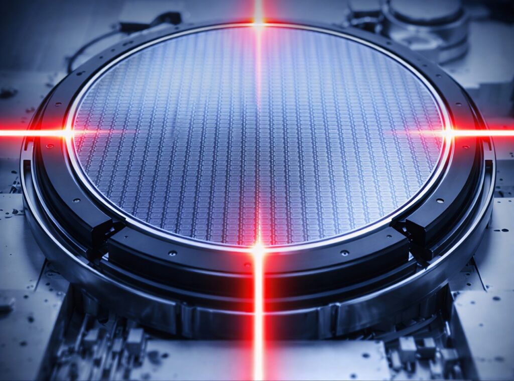
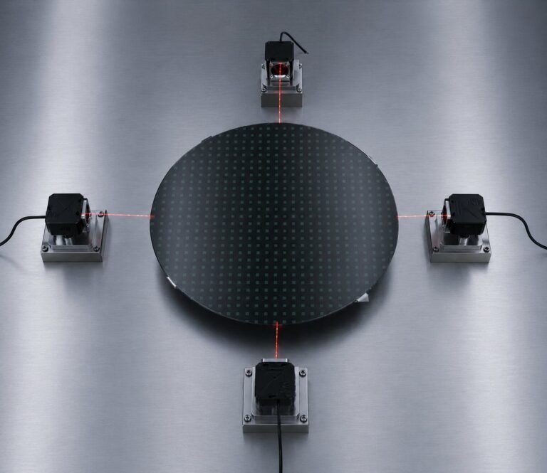
Laser interferometers measure translation, elongation and tilt directly at the object.
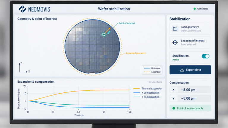
Separates drift, thermal expansion and tilt in real time.
FPGA feedback corrects the position before drift ruins the sample or the process.
Proven in the lab. Moving towards industry.
From the lab to the demonstrator – measured, documented and open for discussion.
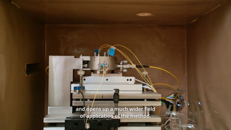 2020–21 · COMPLETEDProof of concept – in the lab
- 0.6 nm RMS residual deviation, held for 10 min per setpoint
- 5 setpoints from 1013 nm down to 140 nm
- 1D lab setup, verified independently by white-light interferometry
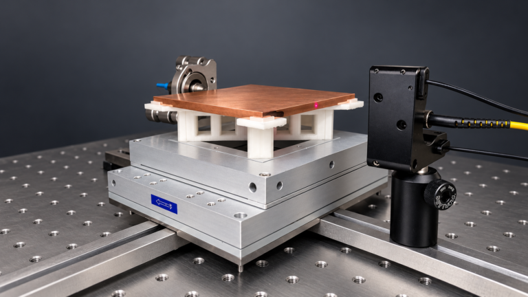 2026 · STATUS QUO · PRELIMINARYPre-demonstrator
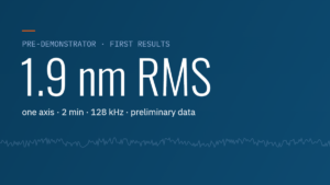
- 1.913 nm RMS after linear trend removal, over 2 min
- 128 kHz sampling in this run – measurements at up to 520 kHz technically demonstrated
- 1 axis – preliminary data, validation campaign follows shortly
- Automated alignment procedure working
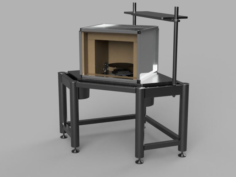 COMING SOONDemonstrator
- Multi-axis control – integrating the controller for active compensation across the multi-axis setup
- Predictive grid – a predictive model of sample displacement that anticipates motion at the point of interest and guides compensation
- In-situ position referencing – an absolute position reference for x, y and θz (rotation about z) directly within the measurement setup
Technical news
MEASUREMENT · OCT 2026
First pre-demonstrator results: 1.9 nm RMS
First tests on one axis – and already promising. Validation campaign to follow.
RESULT · 2020–21
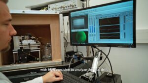
Sub-nanometer stability: 0.6 nm RMS over 10 min
How we measured the proof of concept – and what it does not show yet.
Note: the proof of concept was designed for maximum stability on a fixed geometry. The pre-demonstrator is built for maximum flexibility – its stabilization is already running and will improve further as we optimize it.
One platform, several applications.
Wherever heat and motion shift a sample by nanometers, NeoMovis can measure and correct it. Our current focus is bonding – we believe this is where we add the most value today.
What NeoMovis offers
Sensor platform
Interferometric sensors mounted on the sample holder or on the stage – measuring where the error matters.
Thermal expansion, measured
Thermal expansion of sample and holder is measured directly and separated from motion – in real time.
FPGA readout
All channels read out at high resolution, with full access to the raw data.
Tailored closed loop
A control loop calibrated to your system, acting on the point of interest.
IN DEVELOPMENTAbsolute positioning
x, y and θz (rotation about z) – or the axes your process needs – referenced absolutely for the sample or point of interest.
IN DEVELOPMENTPredictive modelling
Anticipates sample displacement before it happens and guides the compensation.
CURRENT FOCUS
Advanced packaging: wafer-to-wafer bonding
Already working: an automated alignment procedure and in-situ measurement directly on the sample – very fast thanks to FPGA-based signal processing.
In development: complete alignment directly in the bonder – x, z and θz (rotation about z) – with nanometer precision and at high speed.
We would like to define realistic benchmarks together with bonding equipment makers and process teams.
Also a strong fit for
Lithography & reticles
Keep reticle and wafer position stable while exposure heats the system.
Precision stages
Measure the real position at the object instead of at the encoder.
SPM & metrology
Remove thermal drift from long, high-resolution measurements.
Micro- & nanofabrication
Hold alignment during processes that put energy into the sample.
Working on one of these? Tell us about your setup →
From lab project to company.
Funding, partners and milestones on the way to a NeoMovis spin-off.
- 2020–21Lab proof of concept
- 2022Patent filed
- 2026 · todayPre-demonstrator
- 2027Industrial pilots
- 2028Product & spin-off
News & events
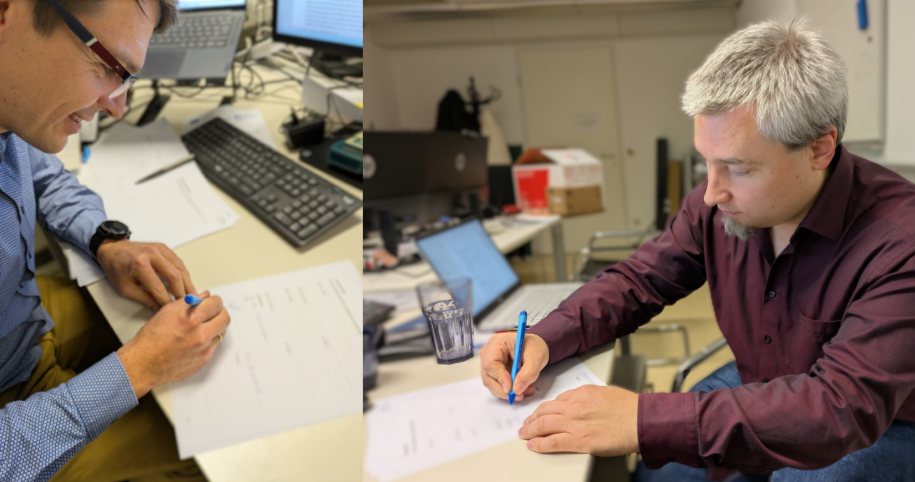 MILESTONE · OCT 2025CDG Transfer.S2S funding granted
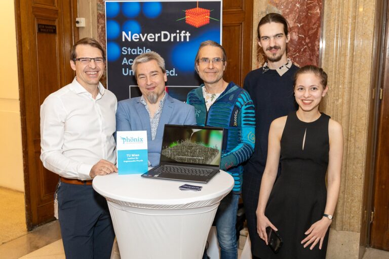 AWARD · 2025/2026Top 3 nominee for the Phönix 2025/2026 award
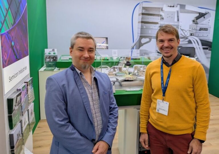 EVENT · NOV 2025Meeting the industry at SEMICON Europa 2025
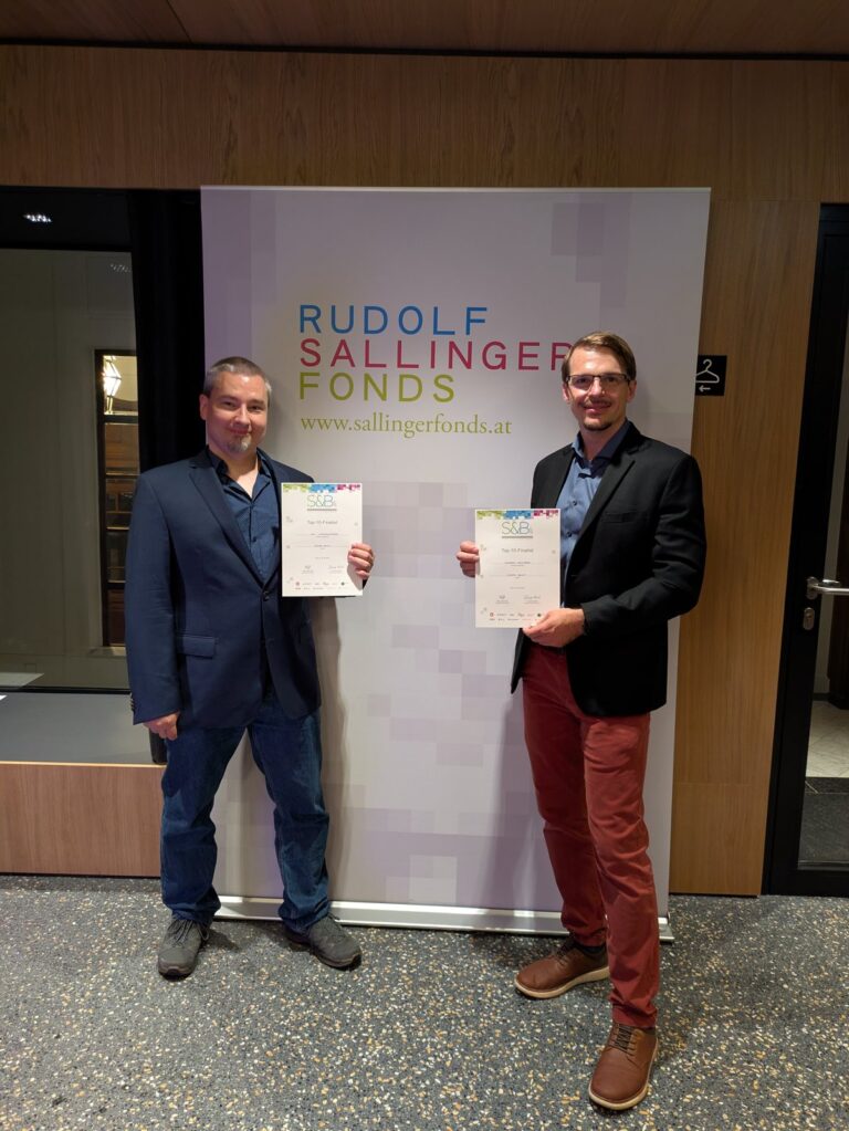 AWARD · MAY 2025Top-10 finalist at the S&B Award 2025
 MILESTONE · NOV 2024The idea of commercialising NeverDrift is born
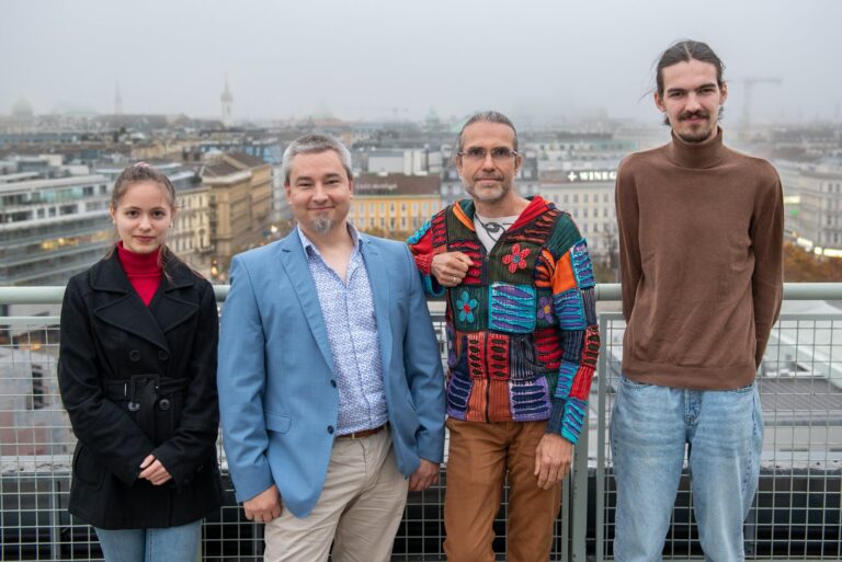 TEAM · EARLY 2025Where it started: the core team
Who is behind NeoMovis

Dr. Michael Hollerer
CEO
Physicist (University of Graz), postdoc at the TU Wien Institute of Applied Physics. Start-up experience at Cellectric – from lab prototype to product development. Leads NeoMovis: strategy, partners and the spin-off.

Dr. Kai Schwenzfeier
CTO
Doctorate at TU Wien (2022) on interferometric measurement, at the Institute of Applied Physics since 2017. Electronics, IT and physics in one person – prototyper and tech specialist who turns ideas into working systems.

Prof. Markus Valtiner
Advisor
Head of the TU Wien Institute of Applied Physics and its Applied Interface Physics group. Opens doors to network and infrastructure.
Supported by a development team of seven researchers, engineers and students at TU Wien. Meet the team →
How a pilot works
Four steps from first call to a test on your own tool.
- 1
Intro call
Your drift or positioning challenge, tool and specifications.
- 2
Feasibility
Fit check under NDA and a joint measurement plan with success criteria.
- 3
Lab benchmark
Measurement at TU Wien on representative sample or stage geometry; report shared with you.
- 4
On-tool pilot
Integration test on your equipment. Then: co-development, license or OEM integration.
Conditions. Steps 1 and 2 are free of charge. A lab benchmark typically takes 6–10 weeks; scope and any cost sharing are agreed per project. On-tool pilots start in 2027. Background IP stays with each party; rights to joint results are agreed before the start.
SUPPORTED BY




Developed at TU Wien, Institute of Applied Physics. Funded by the Christian Doppler Research Association (CDG Transfer.S2S, 2026–2028); earlier prototype funding by aws.
Incubated by the TU Wien i²ncubator, a one-year incubation program for TU Wien affiliated deep-tech innovations run by the TU Wien Innovation Incubation Center.